MBCFET Structure Modeling & Physics
A TCAD-driven device study of the Multi-Bridge-Channel FET (MBCFET), representing Samsung's Gate-All-Around (GAA) evolution of the nanosheet transistor, aimed at understanding the geometric parameters that control the $I_{on}/I_{off}$ ratio and short-channel immunity at sub-5 nm logic nodes.
| Type | Device-level TCAD study |
| Toolchain | Silvaco TCAD (Atlas for device simulation) |
| Target Node | Sub-5 nm logic nodes |
| Key Focus | Short-channel effects (SCE) · DIBL · subthreshold slope (SS) |
Why MBCFET?
As CMOS technology scales down past the sub-5 nm node, the traditional 3D FinFET architecture loses electrostatic control of its channel due to severe short-channel effects (SCE). Gate-All-Around (GAA) architectures, such as stacked nanosheets, restore gate control by completely wrapping the gate oxide and metal gate electrode around the channel. The Multi-Bridge-Channel FET (MBCFET) stacks multiple wide, flat nanosheet channels in parallel. This configuration dramatically increases the effective channel width ($W_{eff}$) within the same footprint, leading to higher drive currents ($I_{on}$) while maintaining low subthreshold leakage ($I_{off}$).
However, the MBCFET design space is highly sensitive to nanometer-scale variations. Parameters such as nanosheet thickness ($T_{ns}$), sheet vertical pitch, gate length ($L_g$), and inner spacer material density must be optimized together to suppress Drain-Induced Barrier Lowering (DIBL) and subthreshold slope degradation.
TCAD Simulation Methodology
This study uses the Silvaco Atlas device simulator to define the 3D device structure and evaluate its electrical characteristics, analyzing carrier transport and electrostatic behavior.
Device Structure Modeling
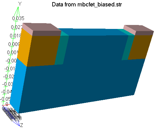
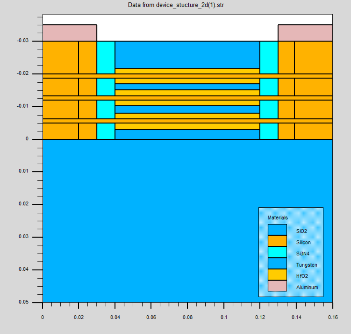
The 3D model of the stacked Gate-All-Around (GAA) Multi-Bridge-Channel FET (MBCFET) is constructed directly in the device simulator with three stacked silicon nanosheet channels, a high-k gate dielectric ($HfO_2$) insulation layer, and a metal gate electrode wrapping completely around the channels.
Structural Design Parameters
The device design space is parameterized to allow systematic exploration of structural components. Key physical dimensions defined in the model include:
- Nanosheet Dimensions: Channel thickness ($T_{ns}$) and effective channel width ($W_{eff}$) defined to evaluate electrostatic volume inversion.
- Gate Stack: High-k metal gate stack wrapping completely around all channel boundaries to ensure maximum gate control.
- Spacer and S/D Regions: Inner spacer geometry and source/drain doping profiles optimized to minimize parasitic capacitances and leakage paths.
Significance
Developing accurate 3D structural device designs in the simulator provides the foundation for electrostatics evaluation at the sub-5 nm nodes. These device models serve as a key reference for studying next-generation Gate-All-Around (GAA) scaling limits, enabling early-stage design-space exploration prior to physical prototyping.